
Contact
VA Contact
VA Innovation designs high-performance contact pins and contact fingers for semiconductor test applications. Our solutions support a wide range of package types, from fine-pitch devices to high-current, high-frequency applications. With experience in Kelvin and non-Kelvin designs, custom contact geometries, and non-magnetic materials, VA delivers reliable electrical performance, long service life, and consistent contact resistance for demanding production and engineering test environments.
VA has developed a comprehensive portfolio of proprietary contact solutions, including Contact Fingers, Flat Fingers, K Pins, KS Pins, KB Pins, KF Pins, KT Pins, and Kelvin contact technologies for advanced semiconductor testing.
Our proprietary contact systems deliver superior electrical performance, longer service life, and optimized signal integrity for today's demanding test applications. From fine-pitch packages to high-current, high-frequency, and high-temperature testing environments, VA solutions are engineered to meet the evolving challenges of the semiconductor industry.
With over two decades of experience, VA continues to innovate and customize contact technologies for IC design validation, engineering characterization, production testing, burn-in, and reliability applications. Our expertise enables customers to achieve higher test accuracy, improved yield, lower maintenance costs, and extended socket life.
Whether your application requires standard pogo pins or a fully customized proprietary contact solution, VA provides the engineering expertise and manufacturing capability to deliver the right contact technology for your test requirements.
Contact
Contact Pins & Contact Fingers
As semiconductor technology continues to evolve, VA Innovation remains committed to developing advanced contact solutions that meet the industry's increasing demands for performance, reliability, and precision. Our extensive portfolio of contact technologies is designed to support a wide range of semiconductor packages and test applications.
Product Portfolio
Probe Pins
- Double-Ended Pins
- Single-Ended Pins
- Kelvin Pins
- Non-Kelvin Pins
Probe PinsVA Proprietary Contact Technologies
- K Pin /KS Pin/KB Pin/KT Pin
- Top Contact Designs
- Side Contact Designs
- Kelvin & Non-Kelvin Configurations
Contact Fingers
- Kelvin Contact Fingers
- Non-Kelvin Contact Fingers
Flat Fingers
- Kelvin Flat Fingers
- Non-Kelvin Flat Fingers
Probe Pins
- Double-Ended Pins
- Single-Ended Pins
- Kelvin Pins
- Non-Kelvin Pins
VA Proprietary Contact Technologies
- K Pin /KS Pin/KB Pin/KT Pin
- Top Contact Designs
- Side Contact Designs
- Kelvin & Non-Kelvin Configurations
Contact Fingers
- Kelvin Contact Fingers
- Non-Kelvin Contact Fingers
Flat Fingers
- Kelvin Flat Fingers
- Non-Kelvin Flat Fingers
Contact
Features & Benefits
VA contact technologies are engineered to deliver reliable performance across a wide range of semiconductor test applications.
Design Flexibility
- Top Contact and Side Contact configurations
- Spring-Loaded and Non-Spring Contact Designs
- Wide Selection of Contact Tip Geometries
- Kelvin and Non-Kelvin Solutions
- Fine Pitch Capability from 0.1 mm to 1.27 mm
Superior Electrical Performance
- Non-Magnetic Contact Options
- Short Signal Path Design
- Low Capacitance, Low Inductance, and Low Contact Resistance
- Optimized for High-Speed and RF Testing Applications
- Excellent Signal Integrity and Measurement Accuracy
Designed for Extreme Test Conditions
- High Frequency Bandwidth up to 100 GHz (-1 dB)
- High Current Kelvin Contacts up to 5 A Continuous per Pin
- High Temperature Operation up to 220°C
Long Service Life
- Typical Contact Life Exceeds 500,000 Insertions
- Selected Designs Capable of More Than 1.5 Million Insertions
- Reduced Maintenance and Lower Cost of Ownership
Contact
Pogo Pins
VA offers a comprehensive range of pogo pin solutions designed to meet the demanding requirements of semiconductor test applications. Available in various tip styles and configurations, our pogo pins provide reliable electrical contact, consistent spring force, and long operational life across a wide range of device packages.
Key Features
Multiple tip styles for different device applications
Stable contact resistance and spring force throughout the product lifecycle
Precision-engineered construction consisting of Plunger, Barrel, and Spring
Available for pitches from 0.10 mm to 1.27 mm
Contact - Pogo Pins
Specifications
VA offers a comprehensive range of pogo pin solutions designed to meet the demanding requirements of semiconductor test applications. Available in various tip styles and configurations, our pogo pins provide reliable electrical contact, consistent spring force, and long operational life across a wide range of device packages.
Barrel
- Brass / BeCu
Spring
- Music Wire
- Stainless Steel (SUS)
Bottom Plunger
- BeCu
Top Plunger
- BeCu
- Hardened BeCu
- SK-4
- Palladium Alloy
- PD Alloy
Available Plating
- Gold (Au)
- PdCo + Au
- Palladium (Pd)
- Rhodium (Rh)
- Crystal Nano Coating
Contact - Pogo Pins
Available Tip Styles
VA offers a comprehensive range of pogo pin solutions designed to meet the demanding requirements of semiconductor test applications. Available in various tip styles and configurations, our pogo pins provide reliable electrical contact, consistent spring force, and long operational life across a wide range of device packages.

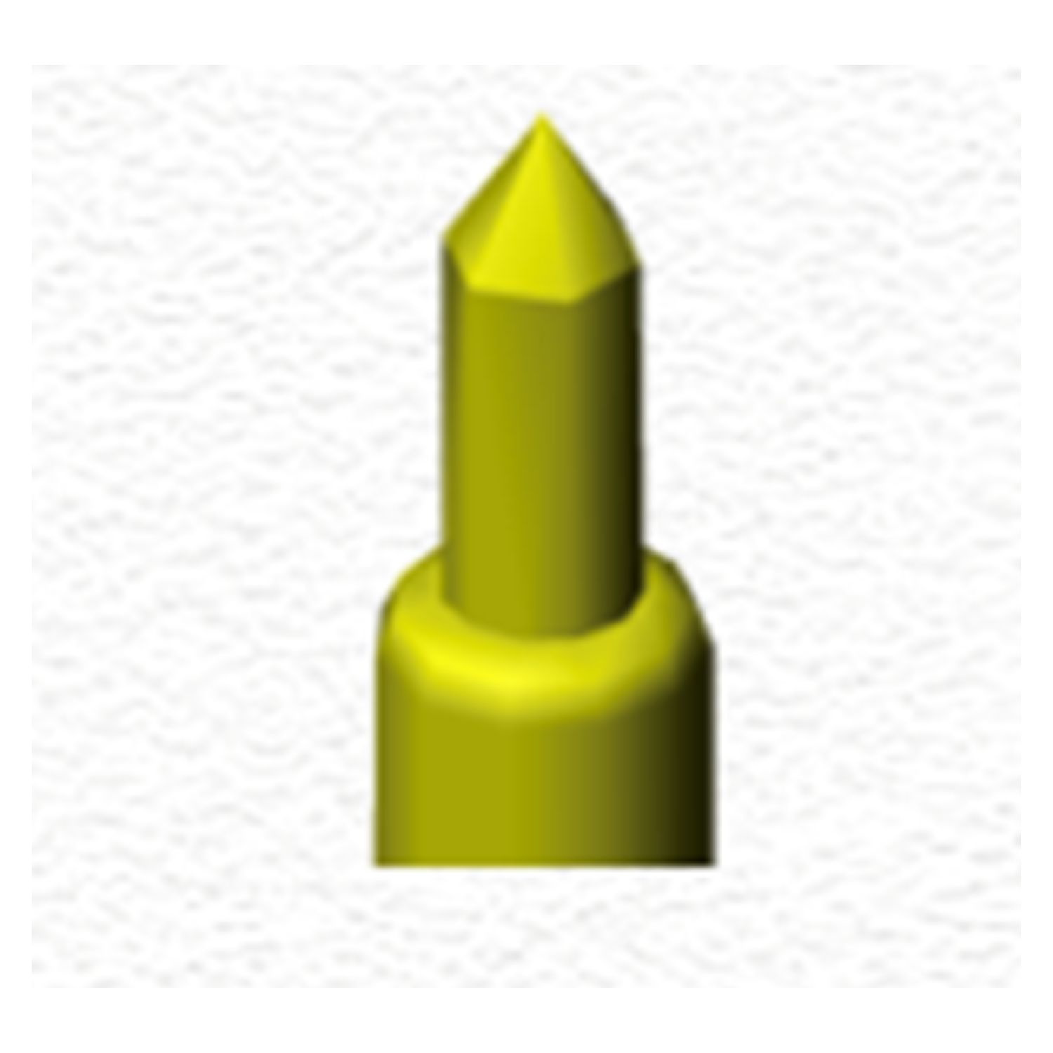
Pointed Tip Concave
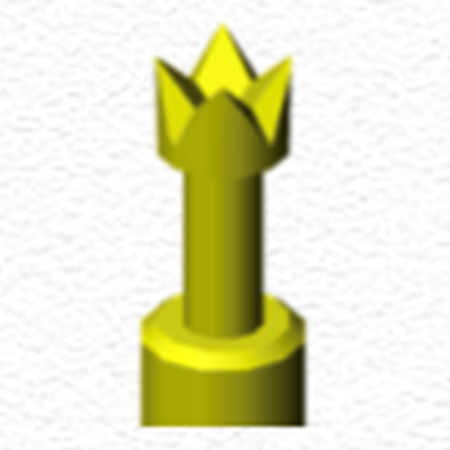
Crown
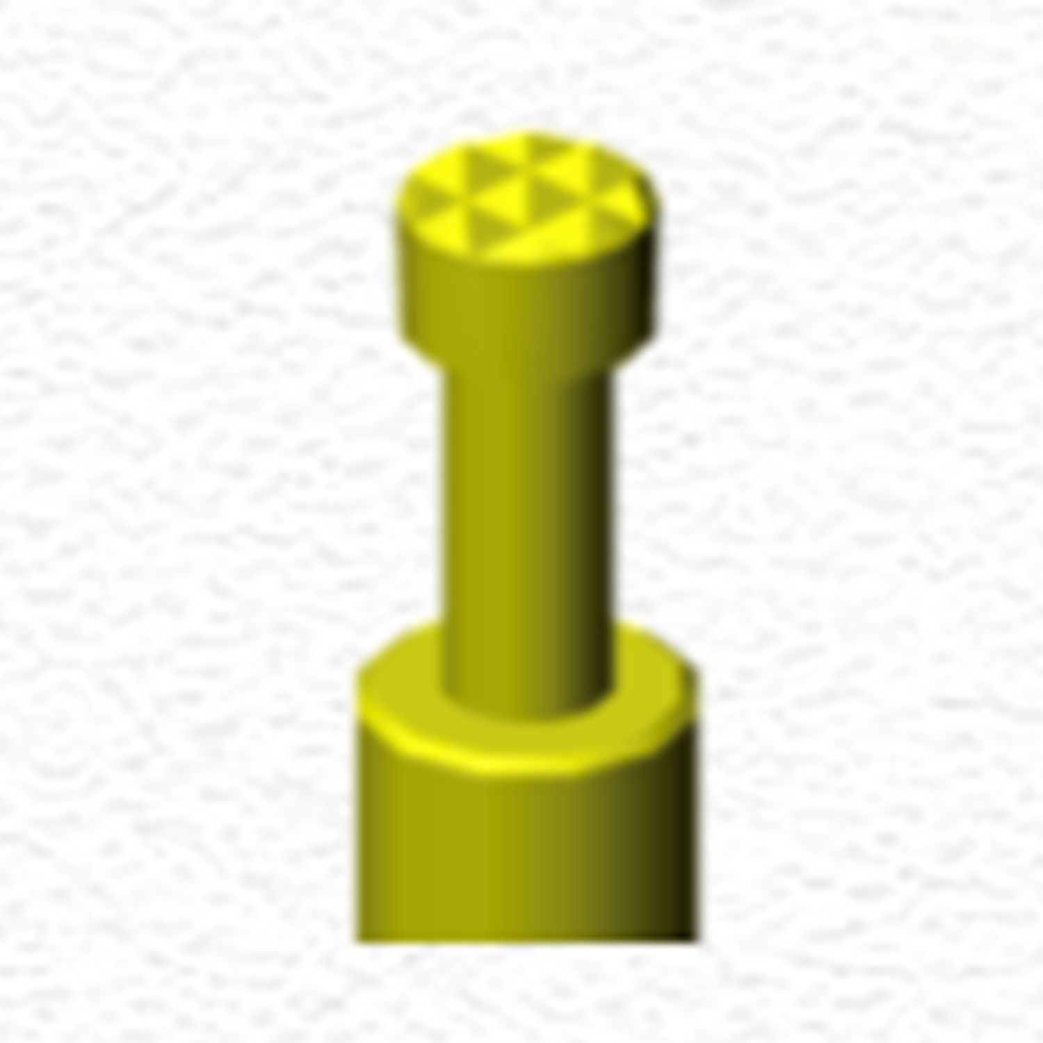
Serrated
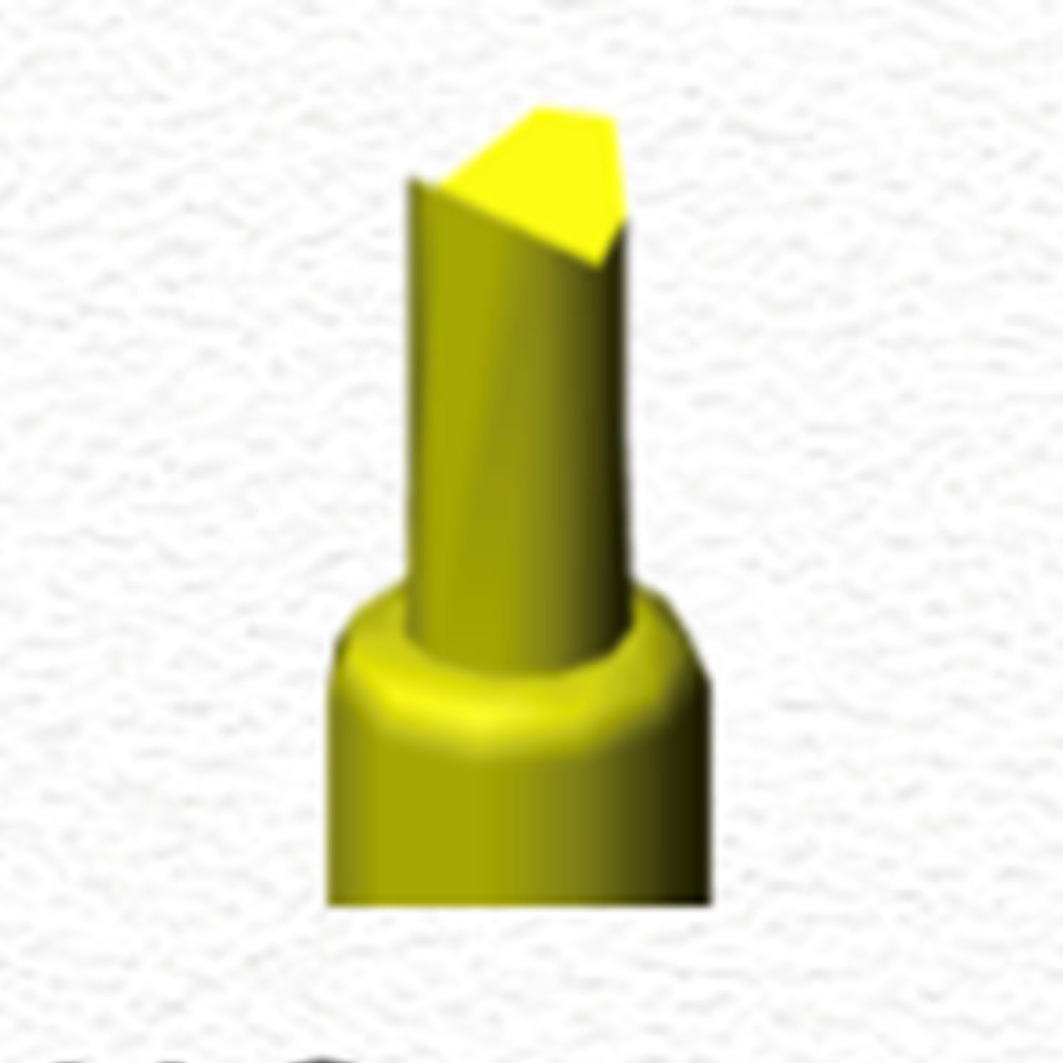
V Cut
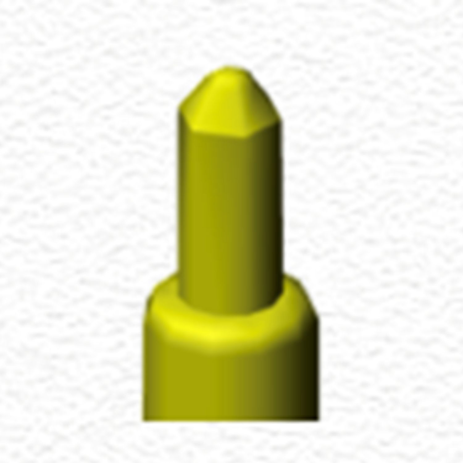
Conical
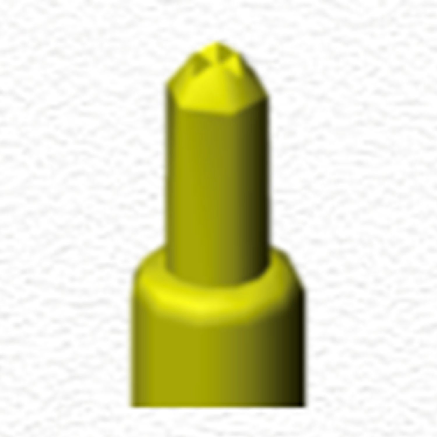
Reduce Crown
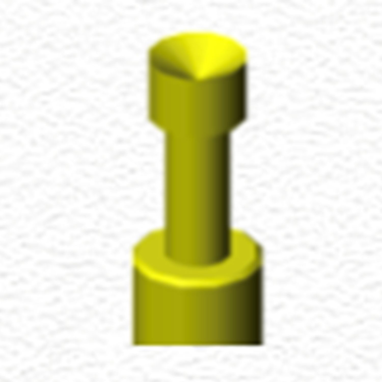
Concave
Contact
VAI - Contact Finger
(Patent pending) Technology
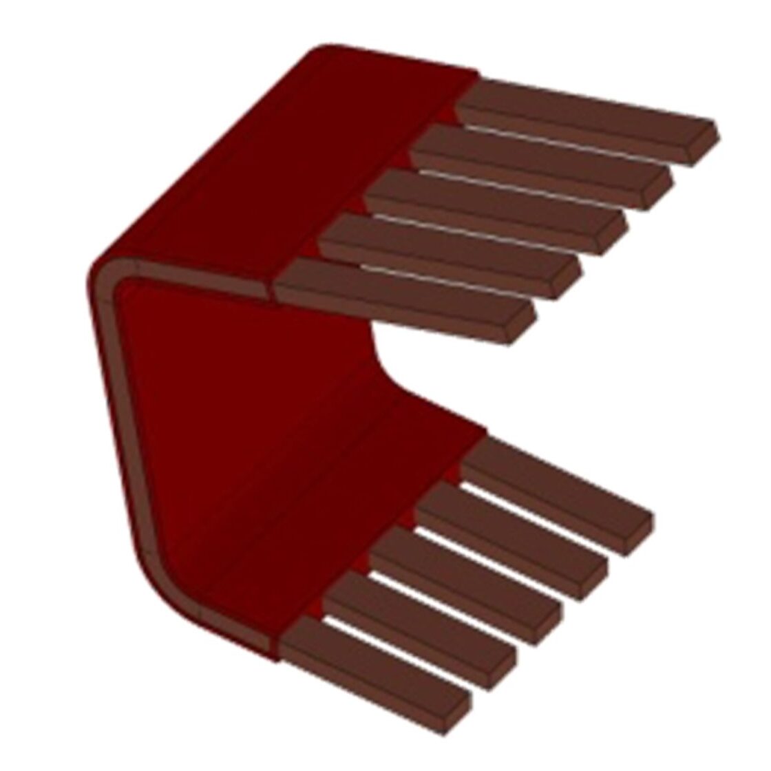
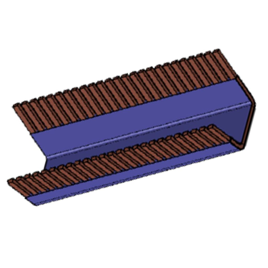
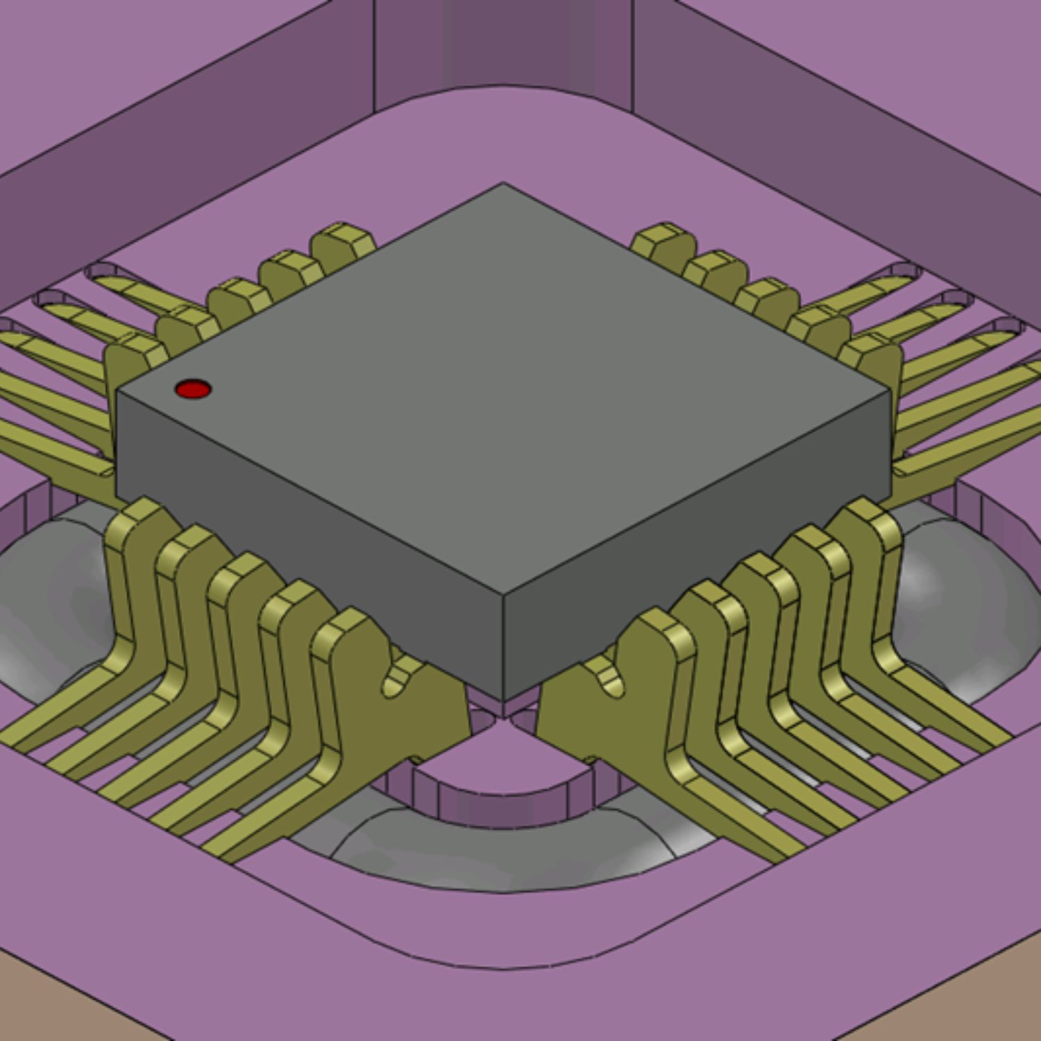
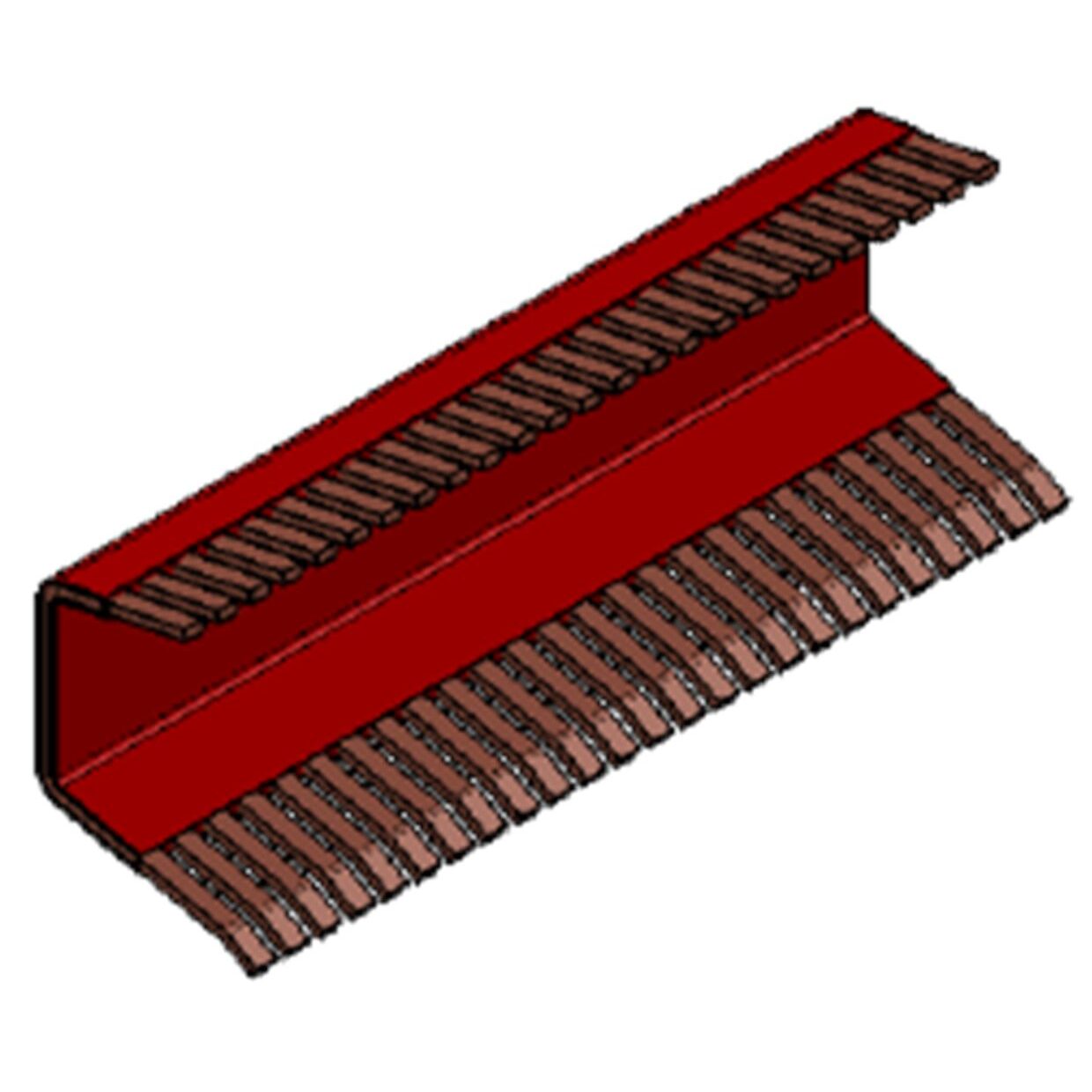
VA Contact Finger ( patent pending ) technology is a proprietary contact solution developed for high-performance semiconductor testing. Each contact finger is custom-designed to match the customer's package geometry, ensuring optimal contact alignment, reliable electrical performance, and long operational life.
Engineered for demanding production and engineering environments, VA Contact Fingers offer excellent bandwidth, low contact resistance, and high current-carrying capability.
Designed to support a wide range of leaded semiconductor packages, VA Contact Fingers provide stable contact performance even under high-speed handling conditions. The modular, replaceable contact finger design simplifies maintenance, reduces downtime, and lowers overall operating costs.
Key Benefits
- Custom-designed to match customer package geometry
- Proprietary VA contact technology
- Excellent bandwidth performance up to 20 GHz+
- Low contact resistance for accurate measurements
- High current capability up to 5.2A continuous
- Low inductance and capacitance design
- Suitable for high-speed and RF test applications
- Supports a wide range of leaded packages
- Reliable performance under high-speed handler operation
- Replaceable contact finger design for easy maintenance
- Reduced downtime and lower cost of ownership
Contact - Contact Finger
VA Contact Finger solutions are widely used in production testing, device characterization, burn-in, and reliability applications where electrical performance, durability, and serviceability are critical requirements
| Electrical Specification | |
|---|---|
| Bandwidth | 20.1GHz |
| Self Inductance | 1.91nH |
| Mutual Inductance (nH) | 0.686 nH |
| Capacitance | 0.659pF |
| Resistance | 27mOhms |
| Max Current | 5.2A Continuous |
| Current Leakage | 714 pA @ 10V |
Replaceable Contact Finger


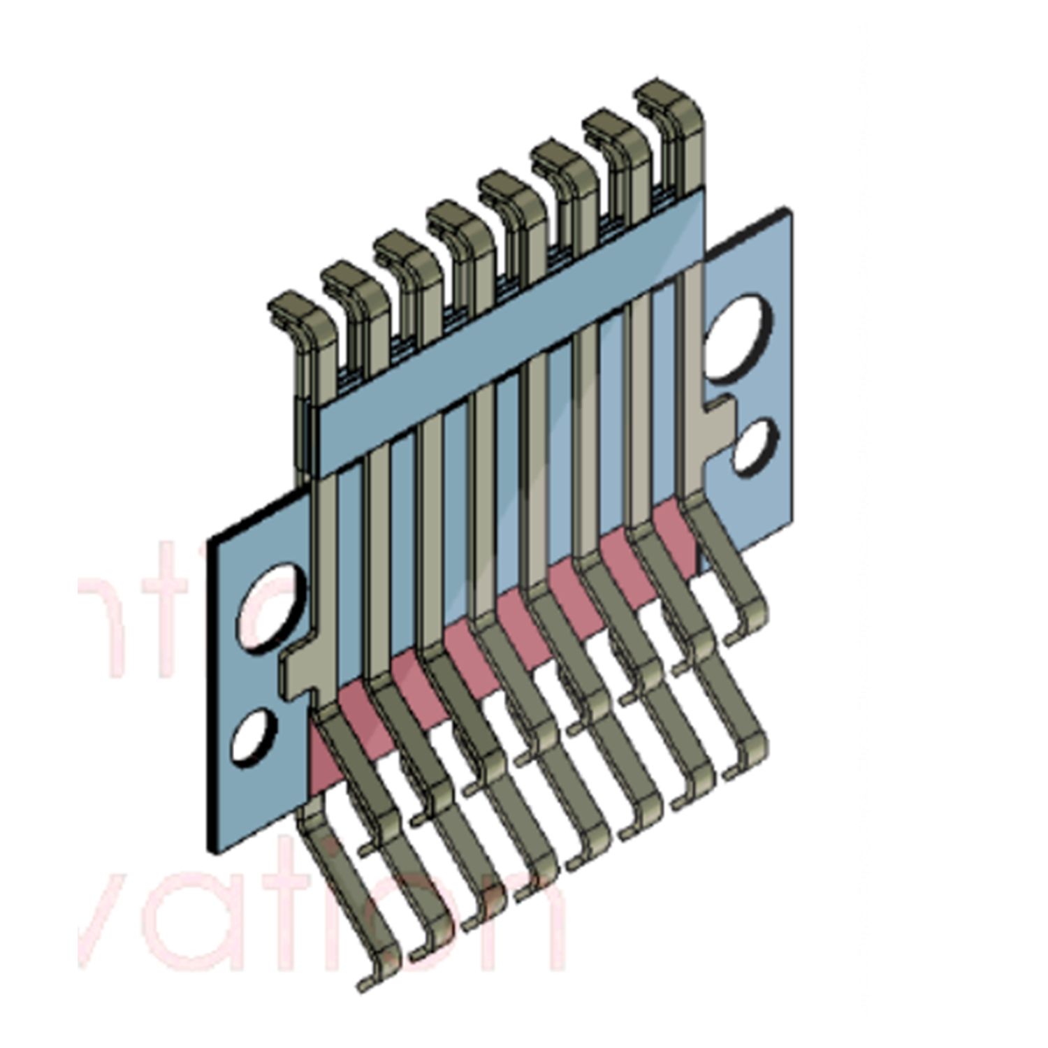
Replaceable Kelvin Contact Finger

Contact
VAI - KT Pin ( Patent Pending) Technology
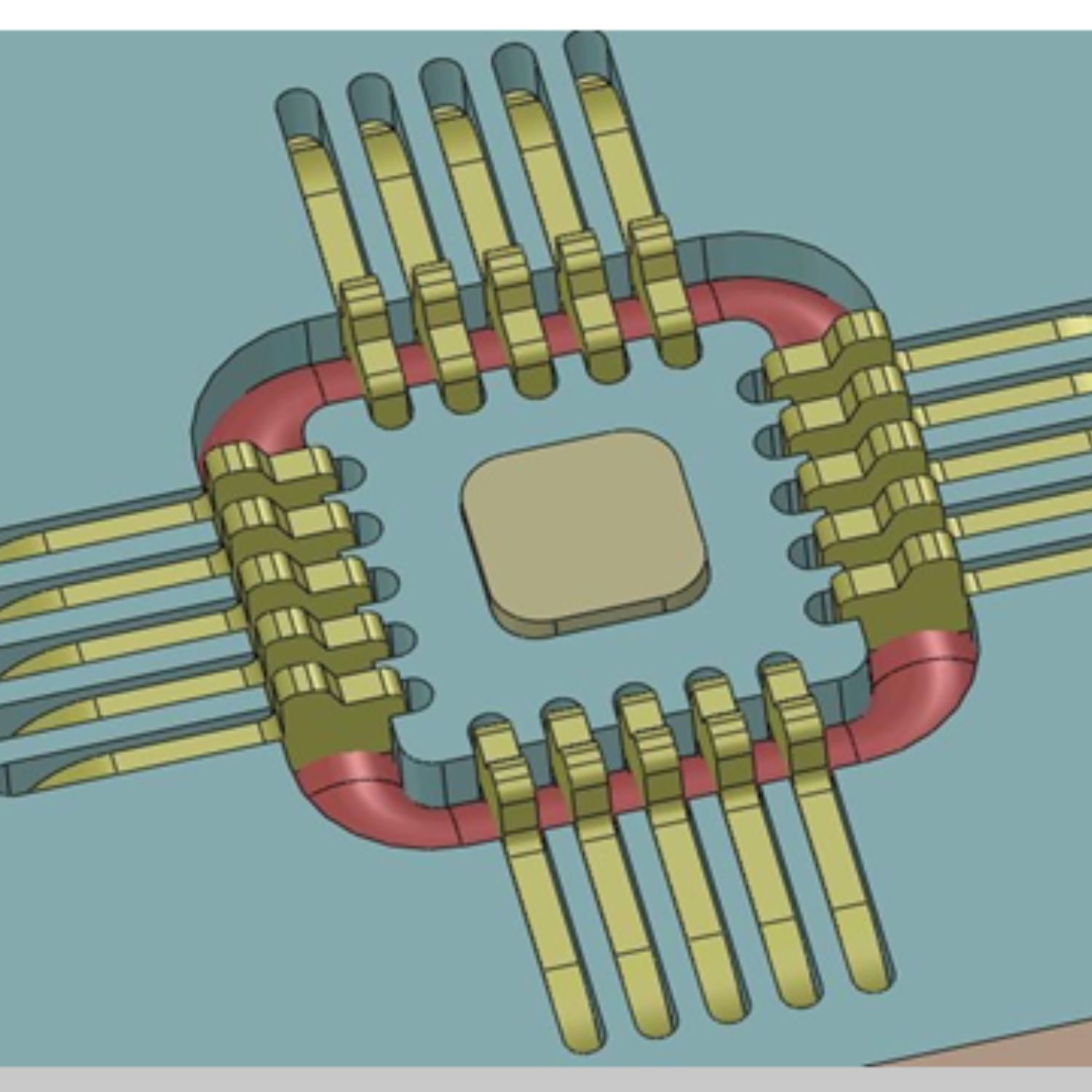
Package Guidance at the Pin Level
The VA KT Pin ( patent Pending) is a proprietary contact technology developed to address the challenges of testing fine-pitch and high-performance semiconductor packages. Unlike conventional contacts that rely primarily on socket-level alignment, the KT Pin™ provides package guidance directly at the contact point, improving package positioning accuracy and contact stability during testing.
Its innovative design combines package guidance and electrical contact into a single contact element, enabling a shorter electrical path between the device lead and test interface. This results in improved signal integrity, reduced inductance, lower contact resistance, and enhanced performance for high-speed and high-frequency applications.
Key Advantages
- Proprietary VA contact technology
- Package guidance at pin level for improved alignment accuracy
- Shorter electrical path for superior signal integrity
- Reduced inductance and contact resistance
- Improved performance for high-speed and RF testing
- Enhanced contact stability during handler operation
- Supports fine-pitch semiconductor packages
- Reduced package movement and contact misalignment
- Suitable for production, engineering, and characterization testing


Contact
Spiral Spring (Patent Pending) Technology
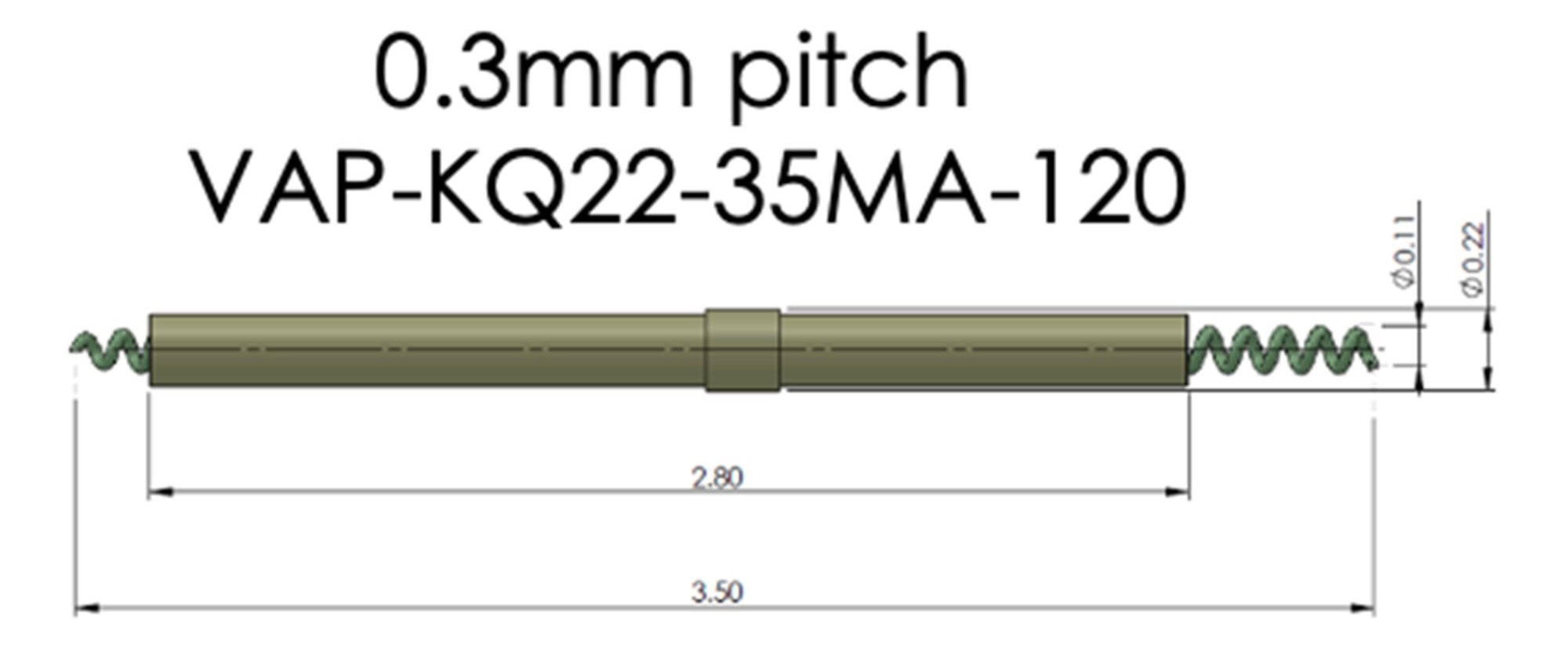
VA Spiral Spring™ is a proprietary spring contact technology , it utilizes a patented spring contact structure that provides larger area of contact and shorter electrical path, improved signal integrity, and superior contact reliability.
Its unique design functions as both a spring element and electrical conductor, creating a highly efficient connection between the Device Under Test (DUT) and the test system.
Contact
KQ (Patent Pending) Pin Technology
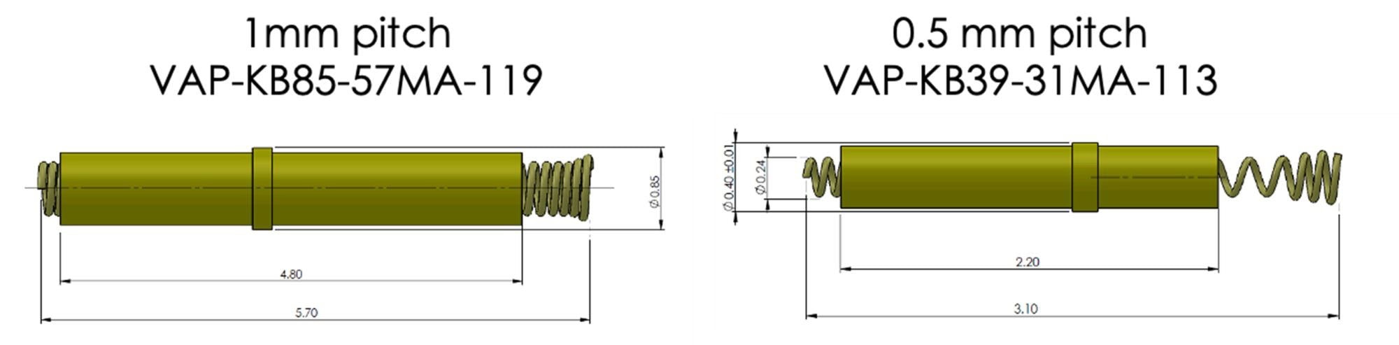
The Next Generation of Spiral Spring Contact Technolog
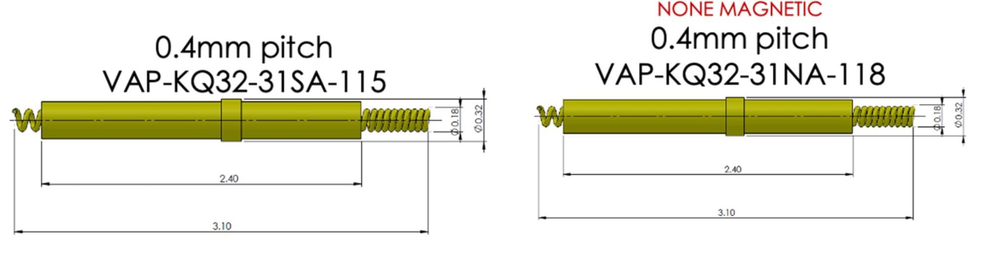
The VA KQ™ Pin is a proprietary contact technology developed from VA's proven Spiral Spring™ concept. By integrating a precision barrel structure with the spiral spring contact, the KQ™ Pin combines the compliance and large contact area of a spring contact with the durability, alignment, and mechanical stability of a traditional contact pin.
Key Benefits
- Low cost
- Larger contact area than conventional point-contact pins
- Accommodates variations in solder ball and pad sizes
- Improved contact reliability and consistency
- Low contact resistance (<30 mΩ)
- High current capability up to 5.1A continuous
- Suitable for test and burn-in applications
- Available in non-magnetic versions
Spiral Spring™
- Large contact area
- Flexible compliance
- Multi-ball-size capability
| Electrical Specifications | |
|---|---|
| Bandwidth | 10.8GHz @ -1dB |
| Self Inductance | 1.27nH |
| Mutual Inductance (nH) | 0.38 nH |
| Capacitance | 0.49 pF |
| Resistance | <30 mOhms |
| Max Current | 5.1 Amp Continuous |


Contact
KS Pin Technology
Flexible Contact Solution for Offset Footprints
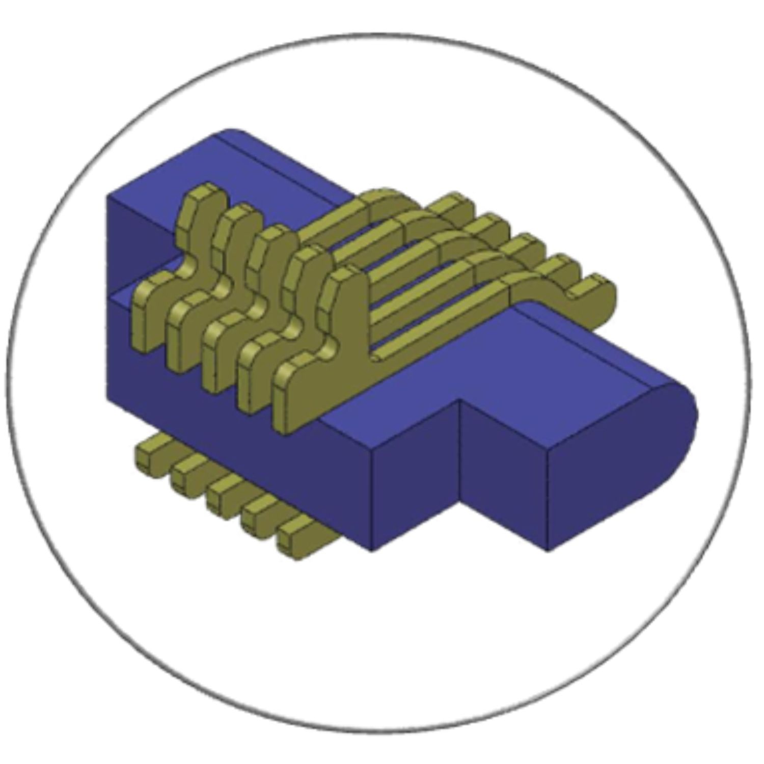
VA KS™ Pin is a proprietary contact technology specifically developed for semiconductor packages with offset or non-standard footprints. Unlike conventional vertical or horizontal contact designs, the KS™ Pin can be customized to match the customer's existing package layout and socket footprint, minimizing redesign requirements and accelerating implementation.
Its unique spring geometry provides excellent compliance and contact force while maintaining a short electrical path for superior electrical performance. The single-piece design offers a simple, robust, and cost-effective solution for applications where footprint constraints or package geometry make traditional contacts unsuitable.
Key Benefits
- Proprietary VA contact technology
- Designed for offset and non-standard footprints
- Custom geometry to match existing customer footprints
- Eliminates or minimizes package footprint redesign
- Single-piece contact design for improved reliability
- Larger contact area for enhanced electrical connection
- Better contact stability and consistent contact force
- Low contact resistance (<20 mΩ)
- High current capability up to 5.1A continuous
- Available in custom sizes and configurations
Electrical Performance
- Bandwidth up to 10.8 GHz (-1 dB)
- Resistance below 20 mΩ
- Self Inductance: 1.27 nH
- Capacitance: 0.464 pF
- Continuous Current: Up to 5.1 A
- Leakage Current: <10 pA @ 10V
Contact - KS Pin Technology
Designed Around Your Footprint
KS Pin – Custom-Matched to Your Footprint, Optimized for Performance
The KS™ Pin is engineered to adapt to the customer's package and socket requirements, rather than forcing the customer to redesign their footprint. This flexibility enables faster deployment, lower development cost, and improved contact performance
Contact
K Pin Technology
Simple, Direct, Cost-Effective Contact Solution
VA K Pin is a proprietary direct-contact technology designed to provide a low-cost and reliable alternative to conventional spring-loaded contacts. Featuring a simple one-piece construction, the K™ Pin eliminates unnecessary components while maintaining excellent electrical performance and mechanical durability.
Its direct-contact design creates a short electrical path between the device and test system, minimizing signal loss and contact resistance. The simplified structure reduces manufacturing cost, lowers maintenance requirements, and enables compact socket designs for high-volume production environments.
Key Benefits
- Proprietary VA contact technology
- Low-cost direct-contact solution
- Single-piece design for maximum reliability
- Short electrical path for improved signal integrity
- Low contact resistance
Electrical Performance
- Bandwidth up to 23 GHz
- Contact Resistance: 30.4 mΩ
- Self Inductance: 2.4 nH
- Capacitance: 0.464 pF
- Continuous Current: 3.1 A
- Leakage Current: 526 pA @ 10V
Contact - K Pin Technology
K Pin – Simple Design, Direct Contact, Lower Cost.
Contact
Contact Finger Technology
Custom-Designed to Match Your Existing Footprint
VA Contact Finger technology is a proprietary contact solution developed for semiconductor test applications requiring superior electrical performance, long operational life, and footprint flexibility. Each contact finger is custom-designed to match the customer's existing package and load board footprint, minimizing redesign effort and accelerating implementation.
Available in both Kelvin and Non-Kelvin configurations, VA Contact Fingers are engineered to provide low contact resistance, high current capability, and excellent signal integrity for production, engineering, and reliability testing.
Unlike standard off-the-shelf contacts, VA Contact Fingers can be tailored to accommodate unique package geometries, lead layouts, and mechanical constraints while maintaining optimum electrical performance.
Key Benefits
- Custom-designed to match existing customer footprints
- Available in Kelvin and Non-Kelvin configurations
- Proprietary VA contact technology
- Low contact resistance for accurate measurements
- Supports a wide range of package types and lead configurations
- Replaceable contact finger options available
- Available in flat finger